
ESDM Business — Backward Integration for Tech Platforms
To make Tech Platforms Portfolio a fully integrated offering as much as Energy Industry, firms must bring in house the EDSM ( Electronics System Design and Manufacturing ) Value Chain. According to the Electronic Industries Association of India (ELCINA), the electronic components market in India has increased from Rs 68,342 crore in 2015–16 to Rs 1,31,832 crore in 2018–19. India’s aspiration to become a major global hub for electronics manufacturing is twofold.
National Challenges
· If we continue to import electronics for strategic sectors and digital platforms/devices, security is an issue.
· So it’s crucial to have design and manufacturing capabilities particularly for critical components which form the basis of storage, memory, processing and interfaces.
· In addition during COVID19, all nations have recognized that even a small disruption of the supply chain can cause severe havoc to the economy of a country.
· With the largest no of electronics items consumed by Indian market, India has a very large industry base of Electronics items, but when we talk about semiconductor inside, we import 95% part of it.
· With the highest level of intelligence man-power & great level of natural resource, why we are not fabricating Semiconductor devices in-house. What are the obstacles to set-up a semiconductor foundry in India.
Why EDSM In India ?
· The world’s fastest growing industry, Electronics System Design and Manufacturing (ESDM) continues to transform lives, businesses, and economies across the globe.
· India is one of the largest growing electronics market in the world
· The global electronics market is estimated to be over $2 tn ( TV — 600 Bn, mobile phones — 495 Bn, personal computers 237 Bn, and datacom products $47.40 Bn and rest others ).
· India’s share in global electronics manufacturing has grown from 1.3% in 2012 to 3.3% in 2020.
· India exported mobile phones worth $1.61 billion to cater to the global demand. But with the NPE https://www.meity.gov.in/writereaddata/files/Notification_NPE2019_dated25.02.2019.pdf goals set at manufacturing 1 Bn phones worth 190 Bn and exporting mobile phones worth $110 billion by 2025, India needs to develop its own component manufacturing ecosystem within the country which will make us less reliant on other countries for imports of components.
· By 2020, the LED market in India is expected to expand to USD 35 billion.
· Digitisation to drive growth in DTH market . By 2020, demand for telecom equipment in India is expected to rise to USD34 billion
· Rising teledensity in the country is leading to higher demand for telecom equipment. By 2020, the semiconductor design market in India is expected to increase with a CAGR of 25.3 per cent to USD60 billion
· India is today World‟s third-largest TV marke. By 2020, the smart television industry in India is expected to expand to USD 27.7 billion.
Changing Indian Scenario
· Technology transitions such as the rollout of 5G networks and IoT are driving the accelerated adoption of electronics products.
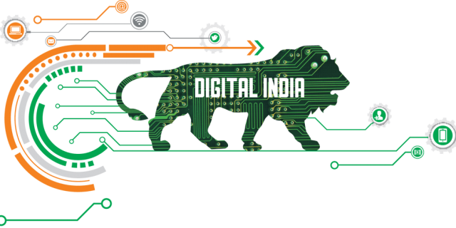
· Initiatives such as ‘Digital India’ and ‘Smart City’ projects have raised the demand for IoT in the market and will undoubtedly usher in a new era for electronic products.
· The wearable & smart electronics trend at our footstep future will influence entire semiconductor industry.
· India is expected to have a digital economy of $1 Tn by 2025
· One of the largest electronics markets in the world anticipated reaching $400 Bn by 2025 from the current Electronics Market of $120 Bn, thereby becoming the fifth largest consumer electronics and appliance industry which would make it a future goldmine of export opportunities.
· Contribution to GDP — 2.5%
· Exports in 2018–19 — $8.8 Bn
· Direct and indirect employment — 13 Mn
· India’s ESDM sector is expected to generate $100–130 Bn in economic value by 2025.
· 100% FDI is allowed under the automatic route.
· In case of electronics items for defence, FDI up to 49% is allowed under automatic route and beyond 49% through the government approval.
Product Segments — The Indian Electronics Sector is split into following product systems. https://www.ibef.org/download/Electronics-March-2015.pdfhttp://www.elcina.com/overview.php
· Consumer Electronics (Mobile Phones, TV, Music Systems).
· Industrial Electronics (UPS Systems, SCADA, PLC, AC Drive Systems).
· Computers (Note-Books, Desk-Tops, Servers).
· Communication and Broadcasting Equipment (Direct To Home DTH, Set Top Box STB).
· Strategic Electronics (Radars, Satellite Based Communications, Internal Security System, Disaster Management System, Drone).
· Electronics Components (Semiconductor Devices, Cathode Ray Tubes, Capacitors, Picture Tubes ).
· Light Emitting Diodes (LED)
· Automotive Electronics.
· Medical Electronics.
Opportunities for Tecch Platforms to meet India’s EDSM Ecosystem Needs
· In semiconductor manufacturing, there are two areas- the wafer fab and assembly testing mark pack (ATMP).
· There is a need to design chips for the domestic market and integrate with the foundry.
· The design, ATMP and foundry have to work parallel to gain headway.
· I strongly believe we should create a full ecosystem, with strong incentives, to go after this. This will entail:
o Creating an R&D facility on the lines of IMEC, Belgium.
o 28nm can be valuable in terms of profitability. There is enough life left for 28nm for the consumption in India across all nodes. India is currently consuming about $1 billion of semiconductors at 28 nm. That is going to remain the same or slightly higher for the next five years compared to 14nm, 10 nm or even 7nm,
o Quickly acquiring second-hand fab of 28 nm, which will take care of a large part of India’s current need, instead of going after the most modern fab; this will not cost more than $500–700 million.
o Alternatively, attract a Samsung-type company within a JV to move existing fab to India.
o Setting up a fab, for Specialty Technologies — GAN, SIC, high-voltage devices, RF, AMS; this will have a good domestic market for inverters, chargers, EV, etc, and will not cost more than $500–700 Mn.
o Strategic partnership to Upgrading the strategic SCL fab to 90/65 nm.
o Attracting at least two assembly-test-mark-pack (ATMP) facilities.
o Creating at least 100 fabless start-ups and giving PLI benefits to them by Govt schemes.
Barriers To Entry In Setting Up Semiconductor facility In India
· Huge Investments Involved
· Semiconductor Fabrication is a volume production facility right from the starting.
· Semiconductor Fabrication will require cheap but skilled labor.
· Very High end world –class machinery involved.
· Requirement of very specific raw materials.
· Uncertain Indian market.
· Customer requirements are changing, and change the electronics inside.
· Disposable of Hazardous Waste
· Infrastructure Requirement
· Lack of education in Indian on Advanced semiconductor manufacturing.
Chips Manufacturing In India
· The Indian chip design industry — including very large-scale integration (VLSI) design — is an integral part of the ESDM ecosystem. Researchers expect that they will be able to manufacture the microprocessor in bulk within a year or two with keeping the cost as little as Rs.100 ($1.50 approx).
· SHAKTI by IIT Madras: SHAKTI is India’s first-ever RISC-V architecture-based microprocessor for smartphones and IoT devices.
· AJIT by IIT Bombay: Engineers from the Indian Institute of Technology Bombay (IIT Bombay) have developed a new microprocessor called AJIT — the first-ever microprocessor to be conceptualised, designed, developed and manufactured in India.
· Pruthvi-3 by Saankhya Labs: It is an improvement over the previous Pruthvi chip (Pruthvi 1) that was launched in 2015, and can be used in multiple communication products including mobile devices, broadcast television, satellite communications, and defence communications. Pruthvi-3 is a fully programmable multi-standard chipset that supports next-generation broadcast standards.
· Unnamed by C-DAC: C-DAC has been entrusted with the mission of the development of an indigenous design of a family of microprocessors, IPs, SoCs and ecosystem supporting the product development to meet India’s requirements for strategic, industrial and commercial sectors. CDAC successfully completed the design, coding, and testing of a series of 64-bit single/dual/quad-core superscalar out-of-order high-performance processors based on RISC-V Instruction Set Architecture, multi-level caches, memory management unit and coherent interconnect.
· Photoresists by IIT Mandi — These are used in the production of printing plates, printed circuit boards, flat panel liquid crystal displays, and magnetic recording heads, but the most important use is in the manufacture of integrated circuit (IC) devices, such as devices of microprocessor for smart electronic chips and gadgets, IoT, AI chips and computer memory chips with high data storage. Improvements in the resolution of what is called the photolithographic process, with the help of photoprotectors, have been key to advances in the semiconductor space. The photoresists are the workhorse for chip manufacturing. Electronic chips are everywhere, including telecommunications, robotics, aerospace, automobiles, railways, defense, and many other strategic and commercial sectors. It has a great impact on the mobile phone industry; the greater the number of transistors on a chip, the better the performance. IIT Mandi is one of the few institutions in India that works for the indigenization of a wide spectrum of sunscreens. In 2012, the institute took up the challenge of bulk production of indigenous photoresist formulations for the Indian semiconductor industries and academic institutes. In 2012, the institute began an initiative for the research and development of futuristic device manufacturing technologies with the support of chip maker Intel, which provided $ 300,000 to develop next-generation materials for 20-nanometer (nm) node VLSI technologies. ). This was demonstrated for 20nm resolution under EUV (extreme ultraviolet lithography) at the Lawrence Berkeley National Laboratory, USA. To put this in context, Taiwan Semiconductor Manufacturing Co (TSMC), the world’s most valuable company in the field, is investing heavily in 5nm manufacturing, is working on a 3nm manufacturing line that will start production in 2023 , and also intends to start the development of a 2nm lithographic process. Currently, the Indian semiconductor industry is involved in 180nm node technology for ISRO. To print these nodes, the Semiconductor Laboratory (SCL) in Mohali uses four different types of photoresists that are sensitive to deep ultraviolet light (DUV). Since no Indian manufacturer develops these DUV resistors, SCL is completely dependent on foreign sellers. The IIT Mandi photoresistor team is working on the development of such DUV resistors.
· Photoresists by SAC Ahmedabad- The Space Application Center (SAC) in Ahmedabad has done some work on 70nm technology at the R,amp;D level. The production capacity for printing wafers is limited in the country.
· Challenges In Chips Manufacturing — The main challenge is
o The lack of indigenous photoprotectors,
o Almost no dedicated test facilities for production on an industrial scale and,
o Less skilled labor.
o More test facilities require large investments.
o Currently, we have very few spaces in SCL’s fabulous line to test products, as the same line is involved in the production of chips. A dedicated facility is needed for testing.
International Standards For Chips — Open Source — The major game-changer
· There are three broad parameters of evaluating are chip — performance, power consumption and size.
· The instruction set (also known as the DNA of a chip) of the SHAKTI microprocessor is an international standard called RISC — V.
· The language to be used by the chip for computation is decided by 20–30 people across the world.
· All the standards are decided by an international committee which guarantees the chip to be at par with anything else out there in the market.
· The contribution of open source technologies has been quite profound with the introduction of open-source EDA tools helping engineers design chips quicker and in an inexpensive manner.
· With the introduction of open-source architecture like RISC-V and so on, the involvement of open source in electronic chip design has become even more impactful.